-
-
-
-
-
-
-
-
South Asia Broadcasting Transmission Silicon Photonics Technology Hot Selling Model
Silicon photonics has developed into a mainstream technology driven by advances in optical communications. The current generation has led to a proliferation of integrated photonic devices from thousands to millions-mainly in the form of communication transceivers for data centers. Products in many exciting applications, such as sensing and computin. Figure 1 maps the evolution of silicon photonics1,2. Silicon-based photonic integrated circuits (PICs) were introduced in 19853 and low-loss waveguides in a thick silicon on insulator (SOI) process demonstrated in 1991–924,5. Various optical devices were next demonstrated6, and soon, silicon photonics was in the small-scale integration (SSI) era—with 1-to-10 components on a PIC. They included demonstrations of high-speed pn junction modulators7,8,9 and photodetectors (PDs)10,11,12,13, as well as heterogeneous integration of a III-V laser to a silicon PIC14. The next era ushered in the commercial success of silicon photonics. With 10-to-500 components on a PIC, this medium-scale integration (MSI) era saw successful demonstration and adoption of Mach-Zehnder modulator (MZM) in intensity-modulated direct-detect (IMDD) transceivers within data centers—both single-wavelength15 and multi-wavelength16,17,18,19. Microring-modulator (MRM)-based IMDD transceivers (see Fig. 2a) demonstrated the multiplexing and energy-efficiency benefits of PIC technology20,21,22. Coherent transceivers in silicon photonics/electronics platforms proved that the technology could compete in performance with their LiNbO3 photonic and III-V electronic counterparts23,24,25. Besides communications, silicon photonics also found new applications such as evanescent-field biosensors26. Silicon photonics is now embarking on the next era of large-scale integration (LSI)—towards 500-to-10,000 components on th. Through the generations of CMOS process development, many materials were added to silicon to reduce the Power, improve the Performance, and shrink the Area—often called the PPA metrics. The additions include Al and Cu for metal traces, Ge for inducing strain and enabling heterojunction BJTs, and silicon nitride (SiN) for passivation and diffusion barriers. The CMOS R&D budgets and commercial markets are orders of magnitude larger than for silicon photonics, so it is natural for silicon photonics foundries to learn from and adopt the innovations from CMOS processes. Hence, we have seen a similar trend in silicon photonics process development. Besides p/n dopants for high-speed modulation, two materials that are now natively supported by several foundries are (1) Ge high-speed photodetectors43, and (2) SiN to expand the wavelength range, enable higher optical power, and support waveguides with lower loss and better phase control in interferometric devices44.Shrinking the area will be a key focus for the next decade of silicon photonics process development for the LSI and VLSI era. In reality, the biggest density limitations rarely come from device size; the spacing between waveguides to eliminate crosstalk is much larger than the size of the actual waveguides. For radio-frequency (RF) devices, spacings between active elements—which are microns in critical dimension—are often in the hundreds of microns, to elimina. Photonics & electronics interplaySilicon PICs almost always exist in conjunction with electronic ICs (EICs). When we look at systems based on photonic chips, the landscape today is almost 100% dominated by data communication, and we expect this to continue for the near future. In this context, EICs serve two purposes (Fig. 2): (1) Enable E/O and O/E conversions of the end-to-end data. (2) Bias, control and compensate for temperature and fabrication variations. Thus, photonics serve electronics by providing the data links, and electronics serve photonics by providing control and readout and digital signal processing (DSP). A major difference between photonics and electronics is that photons don't interact and thus are excellent for transmission of information, whereas electrons interact and repel each other and thus make good switches and computing elements. Each silicon photonic switch therefore requires a corresponding electronic switch. On the whole, the number of transistors in the EIC that must accompany an LSI PIC are orders of magnitude larger than the number of components in the PIC. Here lies a natural interplay, since transistors consume much lower power in (1) switching, (2) providing gain (both linear and limiting), and (3) offering high precision, while being orders of magnitude smaller than the photonic components124. On the other hand, the photonic components (1) enable lower frequency-dependent l. In this section, we describe the top technical impediments to the success of various silicon photonics applications (Table 5), connecting them to some of the challenges and opportunities discussed in previous sections. We limit the impediments to PIC/EIC technology only, excluding economic, regulatory, market, and other factors such as chemistry, biomarkers, quantum advantage, etc. We also do not delve into the benefits of silicon photonics for these applications since most of the previous works describe them in detail.Full size tableFor IMDD transceivers (XVRs) to further improve their energy efficiency (pJ/b) and scale to higher data rates, the modulator FoMefficiency needs further reduction, and the −3 dB E/O BW needs to be improved towards 100 GHz. Improving the WPE of lasers is essential for most applications but especially crucial for communication and computing applications. Efficient multi-wavelength light sources are also needed with adequately large power in each wavelength. Low-noise, large gain-bandwidth APDs in O/L/C bands could provide an SNR improvement without significant power consumption penalty, but historically their bandwidth, linearity, noise, and power handling characteristics have prevented their use at the highest bandwidths. Finally, a. -

Joint venture brand high voltage busbar
Linz, 11 December 2025 – HPW Metallwerk GmbH (HPW), a manufacturer of high-performance copper wires for industrial applications, has established a joint venture with BRAND KG (brandgroup) for the joint production of innovative busbars. The joint venture, operating under the name High Performance Busbars, offers the. HPW and Brand KG have set up a joint venture to develop high-performance busbars for EVs, writes Nick Flaherty. Busbars provide a safe HV connection on shorter distances.
Laser Diodes & VCSEL
High-power CW/pulsed laser diodes (808nm–1550nm) and VCSEL arrays for 3D sensing, LIDAR, and optical interconnects.
Silicon Photonics & CPO
Co-packaged optics engines, silicon photonics ICs, and optical I/O solutions for high-density switches and AI clusters.
Optical Transceivers & AOCs
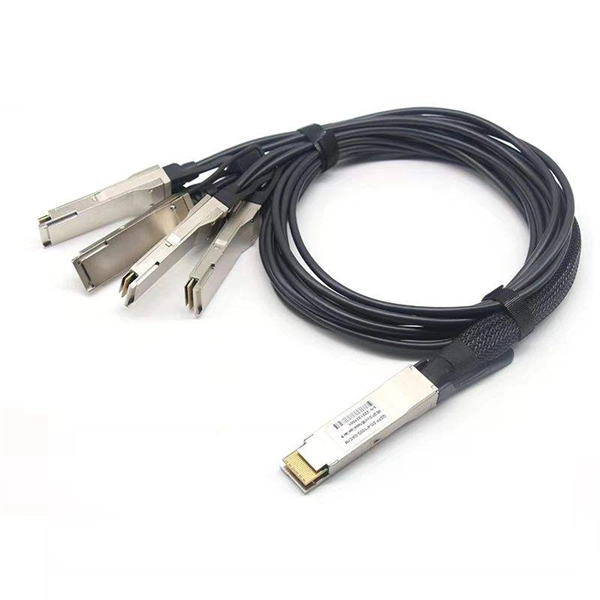
400G/800G QSFP-DD/OSFP modules, active optical cables, and custom optical engines for data center interconnects.
Laser Drivers & CDR
Low-jitter laser drivers, integrated CDR circuits, and linear TIAs for coherent optics and short-reach links.